Cache Bitmap Software and
90nm Cache Failure Resolution
Problem, Analysis, Solution, and PROOF! More Speed + More Yield
Problem, Analysis, Solution, and PROOF! More Speed + More Yield
2003
One of my earlier and proudest development efforts, I taught myself Visual Basic to help analyze the massive amounts of cache data to solve a large problem affecting both yield and operation window.
I developed this software on my own initiative and was singularly able to make sense of the data using custom analytical, graphical, and statistical techniques.
In the end, I was able to provide a single unified theory for the failure that explained all phenomenae and suggest a solution that, once implemented, resolved the issue.
Personal contribution:
- Software Development
- Schematic, layout, and topographical analysis
- Corrective action identification and validation
Recognize There is a Problem
We were suffering from at least a 15% lower yield for a new product design where the failures due to L1 and L2 caches were causing poor operation at low voltage and high speed.
There was too much data and too little information. GB of data on 1000's of die on 100's of wafers.
I could see there was a pattern but couldn't see what it was. So I started writing code to summarize test data into failure signature.
But no-one is looking at the details of the data...
Obvious Failure Dependency:
Blue = L1-D + L2 Caches
Pink = L1-I Cache

Develop Software
Even with summary data, we couldn't SEE the data. So I made the software graphical with interactive query and reporting.
Linking the GDS and Mask databases and adding pattern recognition to the analysis, we could see the wafer-level, die-level, and cache array level patterns.
And they were telling:
Wafer-level - Obvous edge dependent failure rate, even on low fail level wafers. This was a process issue.
Die-Level - Failures were disproportionately higher in L1-I cache than other caches in spite of identical design (but I-cache is wider data bus than D or L2). This is important, but why?
Array-Level - Cache failures occurred at much higher rate on right side of an array but all layout was identical. This is important too, but why?
Bit-Level - Dominant failure mode is "dash-bitline" failure...no fails at high voltage with increasing failure with lower voltage associated with one local data group only. Not defect issue.
Die View when Clicking on Wafer
Allows "Drill-Down" to Deeper Levels

Graphical View of Failures
Across Wafer
Graphical View of Failures
Across Wafer

Obvious Failure Dependency:
Blue = L1-D + L2 Caches
Pink = L1-I Cache

Analyze the Pattern
We were suffering from at least a 15% lower yield for a new product design where the failures due to L1 and L2 caches were causing poor operation at low voltage and high speed.
There was too much data and too little information. GB of data on 1000's of die on 100's of wafers.
I could see there was a pattern but couldn't see what it was. So I started writing code to summarize test data into failure signature.
Close-up View of Individual Fails
Showing Individual Bit Fail Data
Extracted from Test Data

Correlate Data to Design
Correlate Data to Design
I obtained the schematic and layout of the cache design. Failure had to be occurring to the sense-amps associated with local group of bit groups.
Read-0 failing more than Read-1 meant it had to be one side of the sense-amp that failed more than the other...but WHY?
Damage was 'soft'... failures did not occur at high voltage but failed at high rate at low voltage on same die.
Only place that made sense for 0 vs. 1 failure dependency was the bit and bit-bar pass gates. That MUST be it. But HOW?
Bitcell Sense-Amp Pass-Gate
Damage Would Cause Issue
Bitcell Sense-Amp Pass-Gate
Damage Would Cause Issue

Final Correlation...Eureka!
Now I got the actual layout files for the sense amps to study. Using all of the information from the data analysis above, I could focus on differences between design, layout, or placement of pass gates of sense amp. And I found it.
Read-0 pass gate had closer placement to well tie than read-1 gate. If there were to be charge placed equally on the gates of both, it would preferentially conduct on the read-0 side.
All pass gates on all sense-amps across a row of a cache are connected together with a single conductor.
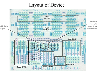
Layout of Sense-Amp
Focus on Geometry Difference of
Sense Amp Pass Gates
Conclusion
Sense amp pass gates for all caches had all gates in a row tied together on a single conductor.
While following process design rules, this LARGE antenna structure would collect charge during wafer processing.
The 'weakest link' of all gates on a given line would conduct excess charge causing weakening of the gate (making it less effective at low voltage)
Layout biased this heavily towards read-0 failures.
Right side of array was connected LATER than left side allowing more opportunity for right side to be damaged during processing.
So...add charge protection feature to this conductor to prevent process charge from collecting and causing damage.
Summary of Root Cause

Proof
After adding feature to prevent charge damage on this conductor, yield improved >15%, speed ratings improved, and the failure mode disappeared. No other design changes were implemented on the cache array design.
Was up-hill battle to convince that this was necessary and I had to develop the software and analysis methods alone due to fab and designers believing that best way to find problem was through physical defect analysis. (charge damage does not create observable physical damage evidence.)
Before (C5XL) vs. After (C5P)
Cache Fail Rates
